

Testhead | Pogo Ring 3 Bottom Board | Y0003ABx Bottom Board | Special Notes | ||||
Pogo Pin | H# | Pin# | Description | H# | Pin# | Description | |
1 | 0 | 1 | CBIT1 | 2 | 1 | CB1 | |
2 | 0 | 2 | CBIT2 | 2 | 2 | CB2 | |
3 | 0 | 3 | CBIT3 | 2 | 3 | CB3 | |
4 | 0 | 4 | CBIT4 - 100k | 2 | 4 | CB4 | |
5 | 0 | 5 | CBIT5 - CLK | 2 | 5 | CB5 | |
6 | 0 | 6 | CBIT6 - WD | 2 | 6 | CB6 | |
7 | 0 | 7 | CBIT7 - STB | 2 | 7 | CB7 | |
8 | 0 | 8 | CBIT8 - RD | 2 | 8 | CB8 | |
9 | 0 | 9 | -5V | 2 | 9 | -5V | |
10 | 0 | 10 | +5V | 2 | 10 | +5V | |
11 | 1 | 1 | VCC RETURN | 2 | 11 | VRTN | Chassis gnd thru power supply board |
12 | 1 | 2 | -12V | 2 | 12 | -12V | |
13 | 1 | 3 | +12V | 2 | 13 | +12V | |
14 | 1 | 4 | +28V | 2 | 14 | +28V | |
15 | 1 | 5 | FIXTURE S/N | 2 | 15 | S/N | |
16 | 1 | 6 | SPARE | 2 | 16 | SP | Testhead pogo pin is removed |
3AB board H2 pins 17-20 are no connect | |||||||
17 | 1 | 7 | HI C3 SENSE | 3 | 3 | V3S | |
18 | 1 | 8 | HI C2 SENSE | 3 | 6 | V2S | |
19 | 1 | 9 | HI C RETURN SENSE | 3 | 8 | RS | Defines gnd for the VIs. S/B connected to gnd at the DUT. Hi impedance input. |
20 | 1 | 10 | HI C1 SENSE | 3 | 10 | V1S | |
21 | 2 | 1 | SHIELD21 | 2 | 21 | GND | Chassis gnd thru DB9-16 board (VI-M5) |
22 | 2 | 2 | OP1 (DB9) | 2 | 22 | DB9 | |
23 | 2 | 3 | OP2 (DB10) | 2 | 23 | DB10 | |
24 | 2 | 4 | OP3 (DB11) | 2 | 24 | DB11 | |
25 | 2 | 5 | OP4 (DB12) | 2 | 25 | DB12 | |
26 | 2 | 6 | OP5 (DB13) | 2 | 26 | DB13 | |
27 | 2 | 7 | OP6 (DB14) | 2 | 27 | DB14 | |
28 | 2 | 8 | OP7 (DB15) | 2 | 28 | DB15 | |
29 | 2 | 9 | OP8 (DB16) | 2 | 29 | DB16 | |
30 | 2 | 10 | SHIELD30 | 2 | 30 | GND | Chassis gnd thru DB9-16 board (VI-M5) |
31 | 3 | 1 | SHIELD31 | 2 | 31 | GND | Chassis gnd thru DB1-8 board (VI-M1) |
32 | 3 | 2 | DB1 | 2 | 32 | DB1 | |
33 | 3 | 3 | DB2 | 2 | 33 | DB2 | |
34 | 3 | 4 | DB3 | 2 | 34 | DB3 | |
35 | 3 | 5 | DB4 | 2 | 35 | DB4 | |
36 | 3 | 6 | DB5 | 2 | 36 | DB5 | |
37 | 3 | 7 | DB6 | 2 | 37 | DB6 | |
38 | 3 | 8 | DB7 | 2 | 38 | DB7 | |
39 | 3 | 9 | DB8 | 2 | 40 | DB8 | |
40 | 3 | 10 | SHIELD40 | 2 | 39 | GND | Chassis gnd thru DB1-8 board (VI-M1) |
41 | 4 | 1 | SHIELD41 | 1 | 1 | GND | Chassis gnd thru VCC5-6 board (VCC-M7) |
42 | 4 | 2 | VCC5 FORCE | 1 | 2 | V5F | |
43 | 4 | 3 | VCC5 SENSE | 1 | 4 | V5S | |
44 | 4 | 4 | VCC6 FORCE | 1 | 3 | V6F | |
45 | 4 | 5 | VCC6 SENSE | 1 | 6 | V6S | |
46 | 4 | 6 | VCC7 FORCE | 1 | 5 | V7F | |
47 | 4 | 7 | VCC7 SENSE | 1 | 8 | V7S | |
48 | 4 | 8 | VCC8 FORCE | 1 | 7 | V8F | |
49 | 4 | 9 | VCC8 SENSE | 1 | 10 | V8S | |
50 | 4 | 10 | SHIELD50 | 1 | 9 | GND | Chassis gnd thru VCC7-8 board (VCC-M11) |
51 | 5 | 1 | SHIELD51 | 1 | 12 | GRD | Chassis gnd thru DP1-8 relay board (VCC-M10) |
52 | 5 | 2 | DP1 | 1 | 11 | DP1 | |
53 | 5 | 3 | DP2 | 1 | 14 | DP2 | |
54 | 5 | 4 | DP3 | 1 | 13 | DP3 | |
55 | 5 | 5 | DP4 | 1 | 16 | DP4 | |
56 | 5 | 6 | DP5 | 1 | 15 | DP5 | |
57 | 5 | 7 | DP6 | 1 | 18 | DP6 | |
58 | 5 | 8 | DP7 | 1 | 17 | DP7 | |
59 | 5 | 9 | DP8 | 1 | 20 | DP8 | |
60 | 5 | 10 | SHIELD60 | 1 | 19 | GND | Chassis gnd thru DP1-8 relay board (VCC-M10) |
61 | 6 | 1 | SHIELD61 | 1 | 22 | GRD | Chassis gnd thru DP9-16 relay board (VCC-M2) |
62 | 6 | 2 | DP9 | 1 | 21 | DP9 | |
63 | 6 | 3 | DP10 | 1 | 24 | DP10 | |
64 | 6 | 4 | DP11 | 1 | 23 | DP11 | |
65 | 6 | 5 | DP12 | 1 | 26 | DP12 | |
66 | 6 | 6 | DP13 | 1 | 25 | DP13 | |
67 | 6 | 7 | DP14 | 1 | 28 | DP14 | |
68 | 6 | 8 | DP15 | 1 | 27 | DP15 | |
69 | 6 | 9 | DP16 | 1 | 30 | DP16 | |
70 | 6 | 10 | GND SENSE70 | 1 | 29 | GREF | Defines gnd for all VCC and VMeas. Hi impedance input. S/B grounded at DUT |
71 | 7 | 1 | SHIELD71 | 1 | 32 | GRD | Chassis gnd thru VMeas board (VCC-M1) DO NOT USE THIS PIN This pin is cut on all standard bottom plates. |
72 | 7 | 2 | VMEAS1 | 1 | 31 | VM1 | |
73 | 7 | 3 | VMEAS1N | 1 | 34 | VM1N | |
74 | 7 | 4 | VMEAS2 | 1 | 33 | VM2 | |
75 | 7 | 5 | VMEAS2N | 1 | 36 | VM2N | |
76 | 7 | 6 | VMEAS3 | 1 | 35 | VM3 | |
77 | 7 | 7 | VMEAS3N | 1 | 38 | VM3N | |
78 | 7 | 8 | VMEAS4 | 1 | 37 | VM4 | |
79 | 7 | 9 | VMEAS4N | 1 | 40 | VM4N | |
80 | 7 | 10 | SHIELD80 | 1 | 39 | GND | Direct to Chassis. Pin is raised on pogo ring |
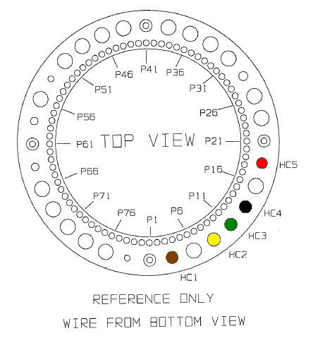
HC1 | HI CURRENT 3 | 3 | 9 | VI3 | 3AB board tied to HC1 and H3 pin 9 | ||
HC2 | HI CURRENT 2 | 3 | 7 | VI2 | 3AB board tied to HC2 and H3 pin 7 | ||
HC3 | ANALOG RET | GND | Direct to chassis. 3AB board tied to mounting screw. | ||||
HC4 | HI CURRENT RET | 3 | 4,5 | VI RTN | Chassis gnd thru VI boards. S/B i return path for VIs. 3AB board tied to HC4 and H3 pins 4&5. | ||
HC5 | HI CURRENT 1 | 3 | 1,2 | VI1 | 3AB board tied to HC5 and H3 pins 1&2 | ||
Notes:
1. If the option does not exist, the corresponding ground may not be present. For example, the gnd thru the VCC7-8 board will only be present if the system contains VCC7 and 8.
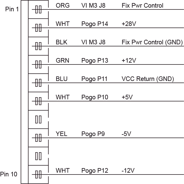
The following diagram is the 10-pin header on the fixture power board inside the testhead
Roos Instruments CONFIDENTIAL AND PROPRIETARY
©2001-2015 Roos Instruments, Inc. All rights reserved.