

| ATTENTION! Limited Availability This RIK is entered Limited Availability with 16 week+ lead times to support old projects. Find the replacement part from the Product Catalog. |
RIK0058A
Two, Dual SPDT RF Switch Modules
The RIK0058A Kit consists of two, dual SPDT RF switch modules, for a total of four SPDT switches. The SPDT Switch is wide band ( DC to 6 GHz) and is intended to be used with the RIK0014A smart carrier. It is especially easy to use since DC wiring is not required when used in conjunction with the smart carrier. It also helps to reduce fixture complexity where RF switching is required.
Top View
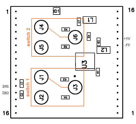
Y0004CC1 SPDT Switch Pin Out
Pin# | Function | DS1 | DS2 | Connector Type |
P2:12 | +5V | Header Pin | ||
P2:11 | -5V | Header Pin | ||
P1:12 | DS1 | Header Pin | ||
P1:13 | DS2 | Header Pin | ||
J1 | SW2 NC | X | 1 | MCX Female |
J2 | SW2 NO | X | 0 | MCX Female |
J3 | SW2 POLE | MCX Female | ||
J4 | SW1 NC | 1 | X | MCX Female |
J5 | SW1 NO | 0 | X | MCX Female |
J6 | SW1 POLE | MCX Female |
Switch 1 & 2 Typical Performance
| Current Drain +/-5V ALL CBITS HI | 100uA Max |
| Current Drain +/-5V 1 CBIT LOW | 500uA typical |
| Current Drain +/-5V 2 CBITS LOW | 1mA typical |
| Insertion Loss (Activated) | Fig. 1 |
| Minimum Freq. | DC |
| Isolation / NC to NO | Fig. 2 |
| Isolation / Pole To Inactive | Fig. 3 |
| Common Port Return Loss | Fig. 4 |
| Active Port Return Loss | Fig. 5 |
| 2nd Harm @13dBm Pin 880MHz | 60dBc |
| 3rd Harm @13dBM Pin 880MHz | 65DBc |
| 1dB Compression | 24dBm |
| Max Inout Power | 33dBm > 500MHz |
| Open Pole | Absorptive |
Coding Requirements:
Fixture Carrier Position# | Smart Carrier Module# |
M1 | M1 (S1) |
M2 | M2 (S2) |
M3 | M3 (S3) |
M4 | M4 (S4) |
M13 | M5 (S5) |
M14 | M6 (S6) |
M15 | M7 (S7) |
M16 | M8 (S8) |
Fixture requirements:
1. Smart Carrier (RIK0014A).
2. Press in connector strips ( 16 pin ) installed at desired module locations ( M1 - M16 ).
3. Bench Top DC Voltage Requirements: +5V / -5V
Cbits Programming:
1. When writing to a Smart Carrier Cbit the format is of S#10XX
- S = S, # = Module number being written to (located at M# on the carrier board)
- Bit position = S# DS1 DS2 DS3 DS4
Examples:
- S3X1XX = routing signal out J1 (Switch2 normally closed) at module location 3.
- S3X0XX = routing signal out J2 (Switch2 normally opened) at module location 3.
- S31XXX = routing signal out J4 (Switch1 normally closed) at module location 3.
- S30XXX = routing signal out J5 (Switch1 normally opened) at module location 3.
S21
Fig. 1
Isolation NC to NO
Fig. 2
Isolation Open to Common
Fig. 3
S11
Fig. 4
S22
Fig. 5