

For latest Cassini information:
| Subject | Web Address (URL) | Type | |
| DIB Design Guide - DUT Interface Board, Device Interface | http://roos.com/docs/RBEH-8STVCB?Open | Cassini Basic Training |
Purpose:
The purpose of this document is to provide the test engineer with guide lines for DIB layout and design. These guidelines are intended to be used with DUT boards to be used on the ROOS standard 12 and 20 RF format test fixture interfaces.
RI recommends a 2 layer thin board to keep parasitics and cost to a minimum. The DUT Board design is intended to be pin for pin straight launching so no internal layers should be required. The RI Test Fixture concept was developed to support higher cost more complex or active components and functions as modules located in the test fixture. Here they are protected and can be reused on many DUT board applications.
The top ( socket side of board ) should have a complete ground plane for noise suppression and to reduce ground inductance at the IC. This ground plane on top along with a conductive pedestal support forms an EMI enclosure to reduce emissions susceptibility of bottom side traces. The Top side should have NO exposed components to maximize reliability. A DUT board should be considered a consumable due to contact wear and so components on the DUT board should be passive to keep the cost low and to assist in minimizing thermal sensitivity while increasing reliability.
Typical Design Rules:
1.) Use 0402s under the part, for close decoupling. All other component should be on bottom side as well.
2.) End all DC traces in a 10uH inductor (noise suppression) and 0.01uF plus optional 100pF (close to dut), caps (shunt). Do not use caps larger than .1uf. Power VI cannot use inductor input (due to sense/limiting)
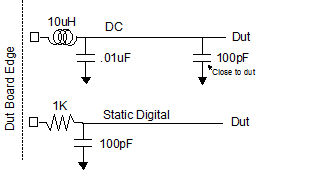
3.) Static digital use 1K Ohm series, 100pF shunt.
4.) You must connect all grounds at single point and that point should be connected to the ground return.
5.) Put in the serial number chip (DS2401) and power for it.
6.) DC trace 8 mil minimum.
7.) DC space 6 mil minimum.
8.) Vias are to be 10mil minimum.
9.) Pads are to be 26mil minimum.
10.) RF trace 15 mil (50 ohm, on 10 mil Duroid). Do not break the ground plane under or over any RF trace.
11.) For low loss precise RF use Rodgers 10 mil Duroid 4003 etc. FR4 is typically used otherwise to 2.5GHz
12.) Use hard contact finger gold, and be very careful on the plating spec.. follow Socket manufactures spec.
13.) The calibration board should be the same layout without matching components.
14.) Carefully locate Pin1. See document Fixture Carrier board Alignment/Orientation for single-site, dual-site, or multi-site
15.) Use layout nomenclature to match the fixture system for easy debug. See document DIB Board Template
16.) If the application must use on-dutboard signal conditioning (i.e., Video/Differential Buffer) then consider routing intermediate signals to pogo pins for calibration purposes.
17.) Document the fixture and dut board with a Fixture Net List\Spread Sheet
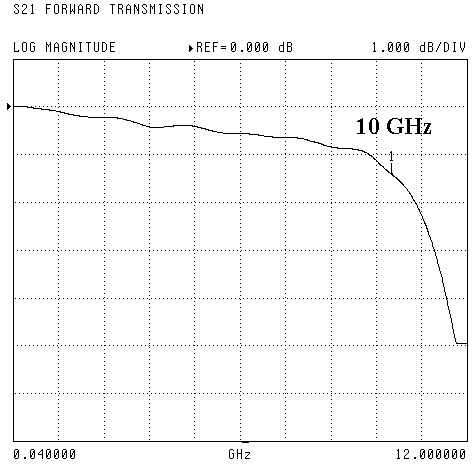
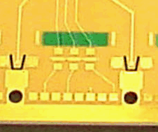
Typical RF Launch Detail for DUT board layout
 |
 |
 |
DC and Shield Placement Details
DC traces must be covered with a solder mask to prevent the shield pedestal from shorting them to the conductive RF gasket material.
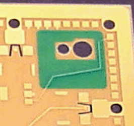
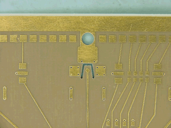
The Serial ID Rom placement is shown here with the corner detail for routing and keepout areas to support the Pedestal mounting. Notice the Solder mask to prevent shorting of the DC traces.
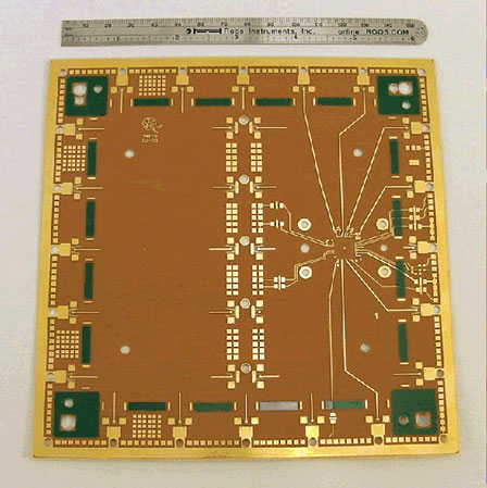
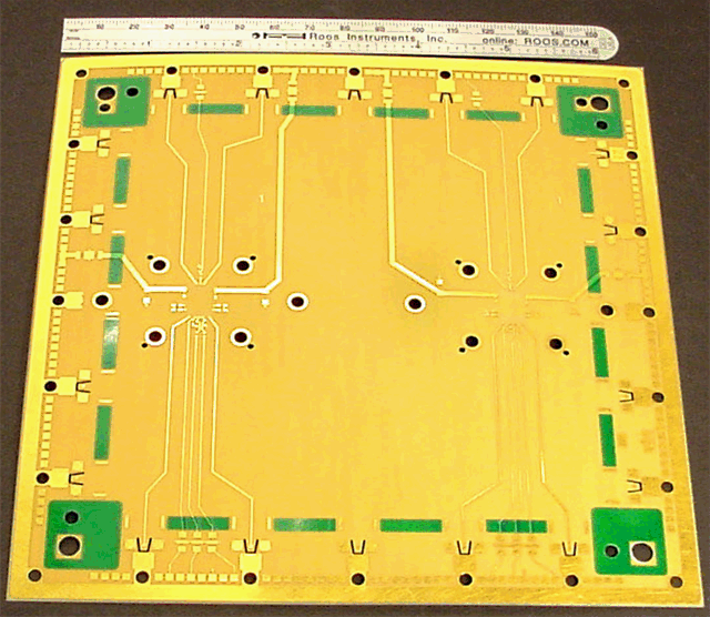
Typical 20 RF DUT board laid out for a Dual Site Application
Template "Gerber" files for 12RF, 20RF, 30RF are available from the online version of this document: http://roos.com/docs/DFES-4QEPS3?Open
12RF DUT Boards
20 RF DUT Boards Gerbers
30 RF DUT Baoards Gerbers
//EDITOR NOTE: ABOVE FILES ARE NOT PRINTED