

1.0 GETTING STARTED
This document describes how to create and edit a serial and parallel ports definition to support the RI Protocol Aware Device Digital Emulation tools.
First, always Log-on to Guru with Test Engineer privilege or above. Refer to Guru Log-on document for details on how to log-on to Guru.
Once you've logged on successfully, launch the Device Control Editor application from the Guru Apps button by selecting Device Control Editor from the Select Application window. Refer to Finding and Launching Guru Applications and ShortCuts document for details on how to launch an application.
2.0 DEVICE CONTROL WINDOW
The RI System Software provides a Protocol Aware vehicle to program the Digital resources into "Single-button" control of a DUT via a Serial or Parallel Bus. This feature allows descriptive names for the serial bus states that mimic or incorporate the device control Protocol into the tester for use during Test Plan Development and drastically reduces confusion and debugging efforts.
Background : Serial Bus Basics: A Serial bus uses 3 or more "wires" or control lines to convey digital information. There is a Clock line that establishes a time reference. A Data line that has the data encoded on it and a Strobe line that establish when the data is valid.
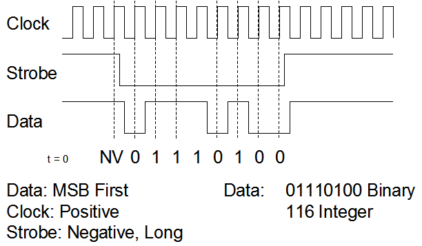
In this case the conventions are MSB first (t=0 on the left). The clock is valid on the positive edge. The strobe is valid low, and is a "long" Strobe meaning it must be low through the whole word. Since the data is MSB first, the data string is 01110100 (MSB>LSB).
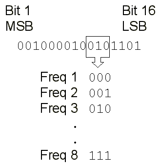
A Serial word contains several fields. These are arbitrary and a function of the design of the bus. In this illustrative case we will establish a 16 Bit bus that has a Frequency control field. This could be for a VCO or some similar function. The frequency filed is defined as 3 bits wide, starting at bit 10. Having 3 bits allows 8 potential states.
RI Naming Conventions
When programming serial bus' in the RI Protocol Aware system there are several conventions to follow:
1.) Bits are named from 1 to N (no bit 0)
2.) MSB is always bit1
3.) MSB/Bit 1 is on the left
Register Addressing
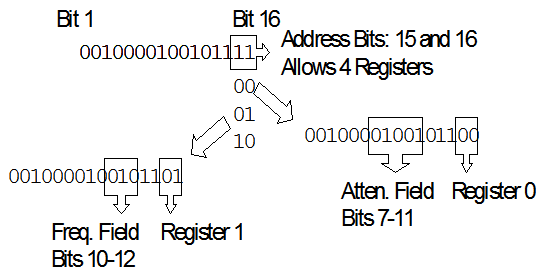
Serial ports can be simple bit changers or have a level of complexity that allow "multiplexing" or register addressing of the serial word to better emulate the device. To illustrate the case, lets look at how several of the serial word bits can be coded as an "address". Since each device register has a unique definition for its own field. So depending on the address a specific bit of groups of bits can have different meanings. This allows a great expansion of the information that can be carried in a small number of bits. In the following example the 16 bit Bus is going to have 4 registers. The last two bits will be the register address. In register 01, bits 10,11 and 12 are the aforementioned "frequency" field. In register 00 bits 7-11 are an "Attenuation" field. Here bits 10 and 11 have different functions depending upon the address.
To Program a Serial Bus:
When building an RI Test Plans, there are two types of Serial bus control that are accepted.
A) The first is a more traditional Local bit control type, which is more "brute force" and involves coding the "ones and zeros" in to the individual Test Panels of the device Test Plan.
B) The second and most powerful is the Protocol Aware "Dut Defined" type which elegantly collapses the programming into a series of single buttons that are automatically generated by the Device Control Editor application and stored into an RI DUT object.
In this document we will concentrate mostly on the Protocol Aware features offered by the "Dut defined" version. We will discuss how the Protocol Aware features pertain to Device Control utilizing the standard built in Static Digital resource that is included in every RI ATE System for basic parallel or serial control operation. The same definitions and Protocol Aware operation is applicable to our Digital TIM as well, and will be discussed later in the section on the Digital TIM operation.
Regardless of the method the Test Engineer chooses to use to control the device, we must define the physical hardware pins that will be utilized in communicating with the Device.
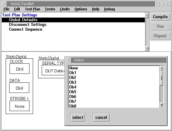
1.) First we must assign the Tester's physical resources: Select the Clock, Data, Strobe and Serial Type buttons from the Static Digital ( or Digital TIM ) control panel and place them in the Global Defaults of your Test Plan.
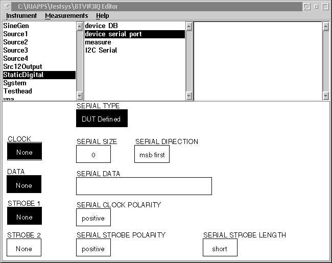
2.) Next select the appropriate DB ( Digital Bit ) lines in this example the CLK is DB1; Data, DB2 and Strobe, DB3.
Now that the physical connections are defined we can manipulate the bits directly in the Test Plan using the following buttons :
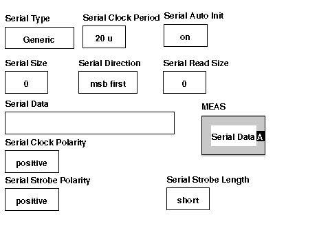
The Serial Data Button is used to enter the binary data that will be sent to the Device. ( i.e. 1001011001 in the following example ) The length of the data stream must be defined using the serial size button. The serial direction and clock period are all defined and are very straight forward to use.

The real issue becomes understanding what the serial stream 1001011001 really means to the device and what mode or operation is selected by this data?????
Even if the Test Engineer commits this to memory, a few weeks or months later the chance of remembering are slim, not to mention unsupportable by anyone else looking at the Test Plan without much more device knowledge.
This is were the protocol aware features of the RI System makes a significant impact.
The serial stream may be made up of several device features that are programmed at once.
The first two bits may be the device mode:
00 = Low power mode
01 = Normal operation mode
10 = High power mode
11 = Test mode
The next three bits may be an attenuation setting:
000 = - 0 dB
001 = - 1 dB
010 = - 2 dB
011 = - 4 dB
100 = - 8 dB
101 = - 16 dB
111 = - 32 dB
The next three bits the gain mode
000 = 0 dB
001 = 1 dB
010 = 2 dB
011 = 4 dB
100 = 8 dB
101 = 16 dB
111 = 32 dB
And the last two the band:
00 = 800 MHz
01 = 1200 MHz
10 = 2200 MHz
11 = 5000 MHz
It will be a big benefit to be able to define ( teach the tester ) the Protocol for control of the DUT
1) The Device Control Editor Application program is the tool that allows the protocol to be entered into the Test System and defined as a specific device. This tool contains all the attributes that define the serial stream just as in the local bit control mode but we embed this into the dut definition and it does not have to added to each Test Plan Global Defaults panel....examples such as :
Serial Style: Serial Standard format, I2C, I3C, SPI etc.
Bit Order: MSB or LSB first
Clock Pulse: Negative or Positive
Strobe: Long or short
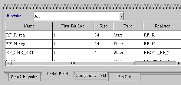
Then each field is defined which represent a logical collection of bits within the register which the user can specify. Each field is represented by a button in the TestPlan editor. The serial field definition consists of:
name -- a unique string for the serial field entry.
first bit location -- indicates the starting point of this field.
register -- which register this field belongs to.
size -- size of the field. The total size for all fields should not exceed the size of a register.
type -- type of field. It can be Constant,Integer, State, UserVar, or Read.
state values -- if the type is set to state, you can enter some state values.
default -- the default state value.
Here we have a field called RF_CNR_RST that is one bit long, starts at the first bit in the register and is a type of "State" like ON or OFF etc.
See the Device Control Editor User's Guide for detailed information on using this tool.
2.) For a more complex device protocol, a register addressing scheme can be supported. This involves creating the field for the address that is shared for all the different addresses. To do this we add an address field. As an example we will name it Reg00_IF_R that is 24 bits long. Importantly, we will make the type Constant, It cannot be state if it is an address. It is constant because in Register 0, these bits are always 00. When they are 01, they are in Register 1 etc..
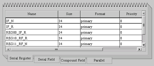
The serial register definition consists of:
name -- a unique string for register name.
size -- the size of the register.
format -- which format does this register use.
priority -- what is the order at which this field will be sent of this register. This field is primarily used by the testplan.
register attributes -- more information for the register in the format of key=value.
3.) Now the fields for each of the registers need to be set up. In this example we will set up the field for attenuation that is part of Register 00.
The name is: Atten
1st Bit Location:Bit 7
Size: 5 Bits
Register : Reg00 (This ties it to the 00 condition for bits 1 and 2)
Type: State
Again see the Device Control Editor User's Guide for detailed information on using this tool.
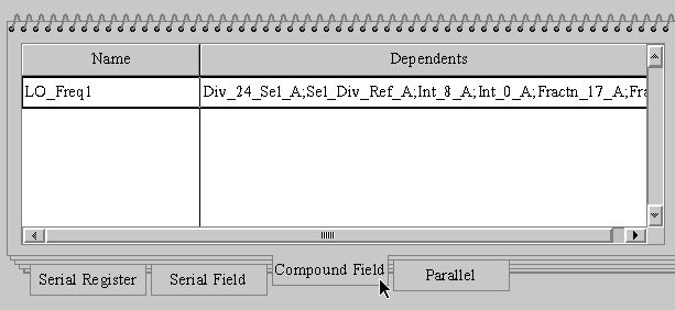
4) For even more complex devices that have many registers, a group or higher level protocol called a Compound register can be defined. It is made up of a combination of multiple registers or fields which are controlled by a single button in the TestPlan. This allows the programming of multiple fields using a single entry which can be very powerful for devices that have high level functionality such as VCO or Synthesisers to realize a function such as set Frequency etc. These values can be imported from a comma separated file into the Compound or edited directly . Compound fields expand into the constituent fields. The compound field definition consists of:
name -- a unique string for the compound field entry.
dependents -- list of field names which have been defined in the Serial Field page.
 .
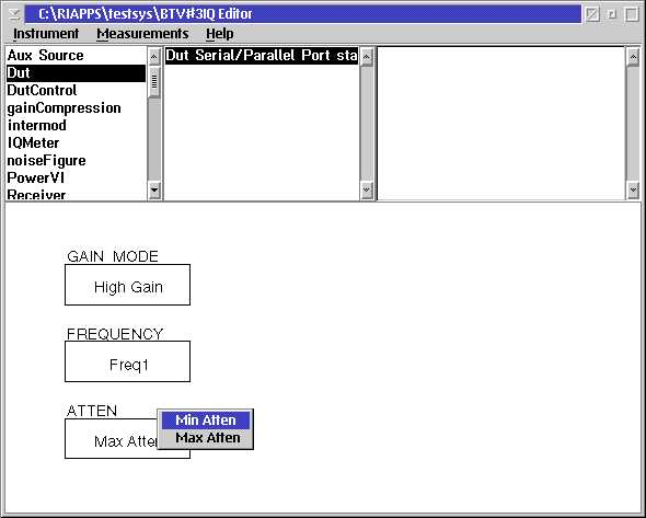
.5.) Upon completion of the Serial Port definition. A DUT object can now be added to the configuration of in the Tester and will show up as DUT>Dut Serial/Parallel Port: These high level buttons are then utilized in Test Plans to control the device.
Serial Bus System Timing:
When utilizing the standard Serial bus control which uses the static digital resource, switches at a 60KHz max Clock rate.
If DB 1,2 & 3 are used exclusively, high speed serial control up to 2.5 MHz clock rate is available.
To implement the fast clock serial:
1.) Special DB line combinations must be used:
Data must be DB2 with Clock DB3 or Data must be DB10 with Clock DB11.